
经典案例
HDI PCB
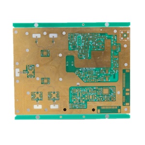
详细介绍
Outstanding Rapid Delivery Capability: Flexible solutions for R&D prototyping, small-to-medium batch, and large-scale PCB design and manufacturing. • Double-sided quick-turn orders completed within 24 hours, multi-layer quick-turn orders within 2-4 days. • Scale advantage for prototypes and small batches: Monthly delivery capacity of over 19,000 variants. World-Class Equipment Capabilities: Producing high-end advanced products including high-layer backplanes, HDI boards, semiconductor test boards, high-frequency boards, high-TG boards, halogen-free boards, rigid-flex boards, and metal-core substrates. --- Standard Rigid PCB Capabilities • Layers: Up to 50 • Board Thickness: 0.2mm – 8.0mm • Max Finished Size: 22.5" × 49" • Min Trace/Space: 3.0mil • Max Aspect Ratio (Thickness to Hole Diameter): 40:1 • Min Mechanical Drill Hole Size: 4mil • Hole to Conductor Clearance: 3.5mil • Impedance Tolerance (Ω): ±3 (<30Ω), ±10% (≥30Ω) • Surface Finishes: Leaded HASL, ENIG, ENEPIG, Immersion Tin, Immersion Silver, Full Board Gold, OSP, Lead-Free HASL, Hard Gold, Soft Gold, Gold Fingers, etc. • Materials: FR-4, High-TG, Halogen-Free, High-Frequency (Rogers, Arlon/Taconic, Nelco, Taixing Microwave F4B, Isola, etc.) --- Rigid-Flex PCB Capabilities • Mass production capability for high-density rigid-flex boards • Layers/Flex Layers: 36 / 10 • Min Trace/Space: 3.0 / 3.0mil • Aspect Ratio: 20:1 • Hole to Conductor Clearance: 6mil • Impedance Tolerance (Ω): 10% • Surface Finishes: Leaded HASL, ENIG, Immersion Tin, Immersion Silver, OSP, Lead-Free HASL, Hard Gold, Soft Gold, Silver Paste, etc. --- Impedance Control & HDI Technology • HDI Capabilities: • 3+C+3: Standard production • 4+C+4: Low-volume + standard production • Laser Blind Via Plating Fill: Standard production • Min Laser Drill Size (mil): 4 --- Metal-Core Substrate Capabilities • Layers: 1-12L (Metal Core & Metal-Clad), 2-24L (Embedded/Metal-Inlay & Cold Plate & Thick Copper), 1-2L (Ceramic DBC) • Board Thickness: 0.5 – 7.0mm | Size: Max: 610×610mm, Min: 5×5mm • Machining Precision: X/Y/Z ±0.03mm (for vent holes, screw holes, etc.) • Thermal Conductivity: • Standard Materials: 1 – 4 W/m·K • Custom Materials: 5 – 12 W/m·K • Ceramic Materials: 24 – 170 W/m·K • Max Copper Thickness for Routing: 28OZ • Metal Surface Finishes: Aluminum Anodizing (Standard/Hard), Chemical Passivation, Sandblasting, Brushing, Electroplating • Surface Finishes: HASL, ENIG, ENEPIG, Immersion Tin, Immersion Silver, Full Board Gold, Soft/Hard Gold Plating, OSP, etc. • Types: Pre-bonding, Post-bonding, Sintering Process, Metal-Clad Core, Embedded Metal Blocks, Cold Plates, Ceramic DBC Boards ---